


The deep neural community fashions that energy in the present day’s most demanding machine studying functions have gotten extraordinarily massive and complicated, pushing the bounds of conventional digital computing {hardware}.
Photonic {hardware}, which may use mild to carry out machine studying calculations, gives a quicker and extra energy-efficient various. Nevertheless, some varieties of neural community computations can’t be carried out on photonic gadgets and require using off-chip electronics or different methods that impede velocity and effectivity.
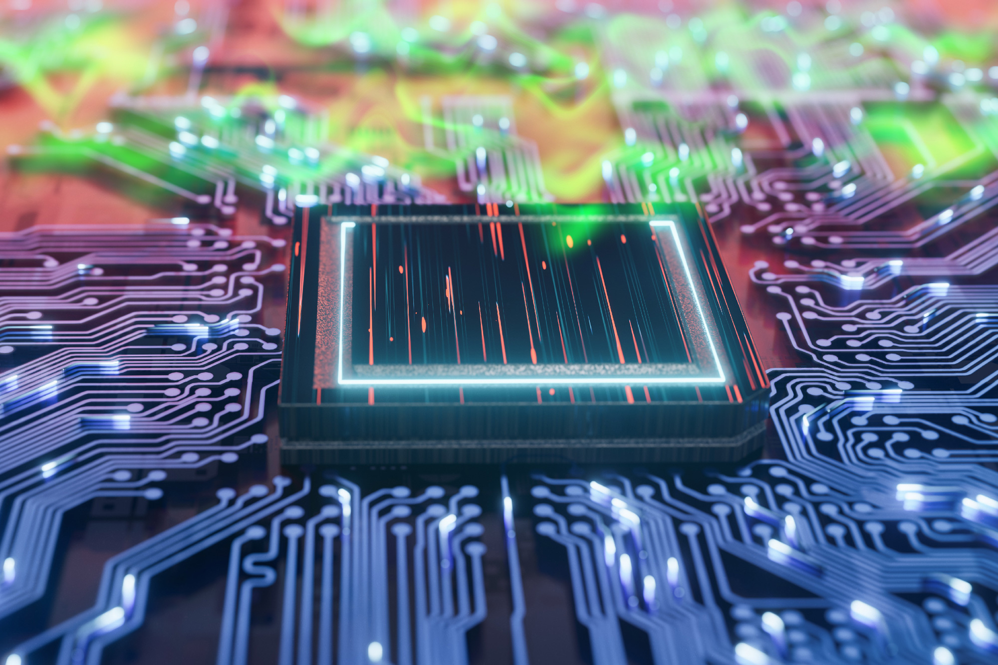
Constructing on a decade of analysis, scientists at MIT and elsewhere have developed new photonic chips that overcome these obstacles. They demonstrated a completely built-in photonic processor that may carry out all the important thing computations of a deep neural community optically on a chip.
The optical gadget was capable of full the important thing calculations for a machine studying classification process in lower than 0.5 nanoseconds whereas attaining greater than 92% accuracy, or efficiency on par with conventional {hardware}.
The chip is made up of interconnected modules that type an optical neural community and is manufactured utilizing a industrial foundry course of, which may probably allow the expertise to be scaled up and built-in into electronics.
In the long run, photonic processors have the potential to allow quicker, extra energy-efficient deep studying for computationally demanding functions akin to LIDAR, scientific analysis in astronomy and particle physics, and high-speed communications. .
“It’s typically not simply how properly a mannequin performs, however how rapidly you will get a solution. Now that we’ve got an finish system, we will begin excited about functions and algorithms at a better degree,” says Saumil Bandyopadhyay ’17, MEng ’18. PhD ’23, Visiting Scientist within the Quantum Photonics and AI Group inside the Analysis Institute of Electronics (RLE), Postdoctoral Fellow at NTT Analysis, Inc., First Creator Paper description of the brand new chip.
Bandyopadhyay is joined on this paper by Alexander Sludds ’18, MEng ’19, PhD ’23. Nicholas Harris PhD ’17; Darius Bunandal PhD ’19; Stefan Krastanov is a former RLE analysis scientist and at present an assistant professor on the College of Massachusetts Amherst. Ryan Hamerly, visiting researcher at RLE and senior researcher at NTT Analysis; Matthew Streshinsky is the previous head of silicon photonics at Nokia and at present co-founder and CEO of Enosemi. Michael Hochberg, President, Periplous, LLC. Dirk Englund is a professor within the Division of Electrical Engineering and Laptop Science, principal investigator within the Quantum Photonics and Synthetic Intelligence Group and RLE, and senior writer of this paper. the examine What will appear today natural photonics.
Machine studying with mild
Deep neural networks encompass many interconnected layers of nodes, or neurons, that manipulate enter knowledge and produce outputs. One of many key operations in deep neural networks is to carry out matrix multiplication utilizing linear algebra. This transforms the information as it’s handed from layer to layer.
Nevertheless, along with these linear operations, deep neural networks carry out nonlinear operations that assist the mannequin be taught extra advanced patterns. Nonlinear operations like activation features give deep neural networks the facility to unravel advanced issues.
In 2017, a gaggle in England, together with researchers within the lab of Cecil and Ida Greene Professor of Physics Marin Soljačić, demonstrated an optical neural community on a single photonic chip that may carry out matrix multiplications with mild. did.
Nevertheless, on the time, this gadget couldn’t carry out nonlinear operations on the chip. To carry out nonlinear operations, optical knowledge needed to be transformed into electrical alerts and despatched to a digital processor.
“Nonlinearity in optics could be very tough as a result of photons do not simply work together with one another. So it’s totally power-intensive to induce optical nonlinearity, so we’re constructing techniques that may do it in a scalable method. It turns into tough to take action,” explains Bandyopadhyay.
They overcame this problem by designing a tool referred to as a nonlinear optical useful unit (NOFU) that mixes electronics and optics to implement nonlinear operations on a chip.
The researchers constructed an optical deep neural community on a photonic chip utilizing three layers of gadgets that carry out linear and nonlinear operations.
Absolutely built-in community
First, their system encodes the parameters of a deep neural community into mild. A collection of programmable beamsplitters, demonstrated in a 2017 paper, then performs matrix multiplication on these inputs.
The information is then handed to a programmable NOFU, which implements the nonlinear operate by siphoning a small quantity of sunshine right into a photodiode and changing the sunshine sign into {an electrical} present. This course of eliminates the necessity for exterior amplifiers and consumes little or no power.
“We keep within the optical area all the way in which to the tip once we wish to learn out the reply. This permits us to attain ultra-low latency,” says Bandyopadhyay.
Reaching such low latency has made it potential to effectively prepare deep neural networks on a chip. This course of is named in situ. Coaching that consumes numerous power, often on digital {hardware}.
“That is notably helpful for techniques that do in-domain processing of optical alerts, akin to navigation and telecommunications, but additionally for techniques that wish to be taught in actual time,” he says.
The photonic system achieved over 96% accuracy throughout coaching assessments and over 92% accuracy throughout inference. That is similar to conventional {hardware}. Moreover, the chip performs key calculations in lower than 0.5 nanoseconds.
“This analysis reveals that computing (in essence input-to-output mapping) could be compiled into new architectures for linear and nonlinear physics that permit essentially totally different scaling legal guidelines by way of computation and required effort. ” mentioned England.
All the circuit was manufactured utilizing the identical infrastructure and foundry processes that manufacture CMOS pc chips. This probably permits chips to be manufactured at scale utilizing confirmed methods that introduce little error into the manufacturing course of.
Bandyopadhyay says scaling up the gadget and integrating it with real-world electronics akin to cameras and communication techniques might be a serious focus of future analysis. Moreover, the researchers hope to discover algorithms that may benefit from optics to coach the system quicker and with higher power effectivity.
This analysis was funded partially by the U.S. Nationwide Science Basis, the U.S. Air Drive Workplace of Scientific Analysis, and NTT Analysis.
